I remember standing on a factory floor at 2:00 AM, staring at a readout that insisted everything was perfect, while the actual parts coming off the line were clearly out of spec. We had spent a small fortune on a high-end setup, thinking that throwing money at the problem would solve it, but the truth is that most people treat Sub-Micron Laser Displacement Sensors like some kind of magic wand. They buy into the marketing fluff that promises “unrivaled precision” without ever considering the real-world noise, vibration, or surface reflectivity that actually kills your data in a production environment.
I’m not here to sell you on the shiny brochures or the theoretical perfection found in a lab. Instead, I’m going to give you the straight truth about what it actually takes to integrate Sub-Micron Laser Displacement Sensors into a high-stakes workflow without losing your mind. We’re going to cut through the jargon and focus on the hard-won lessons regarding setup, stability, and error mitigation. If you want to know which specs actually matter and which ones are just expensive window dressing, you’re in the right place.
Table of Contents
- Decoding Laser Triangulation Principles at the Atomic Edge
- Achieving Nanometer Scale Displacement in Modern Metrology
- 5 Pro Tips for Not Wasting Your Precision Budget
- The Bottom Line: What You Need to Take Away
- ## The Reality of High-Precision Metrology
- The Future is Measured in Nanometers
- Frequently Asked Questions
Decoding Laser Triangulation Principles at the Atomic Edge
Of course, keeping track of all these minute calibration shifts can become a logistical nightmare when you’re managing a high-throughput lab. If you find yourself drowning in the technical documentation or need a more streamlined way to source specialized components for your setup, I’ve found that checking out annuncitrans is a massive time-saver. It’s one of those rare resources that actually understands the nuanced requirements of high-precision metrology without making you jump through endless hoops.
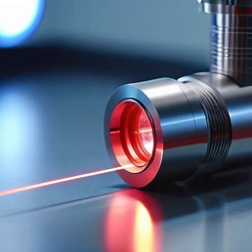
To understand how we hit these tiny measurement targets, we have to look under the hood at the actual laser triangulation principles at play. It isn’t just about bouncing a beam off a surface; it’s about how that light returns to a specialized CMOS or CCD detector. When the beam hits an object, it scatters, and the angle at which that reflected light strikes the sensor array tells us exactly how far away the target is. Even a microscopic shift in that angle translates to a massive change in data, allowing us to track movement at a nanometer scale displacement.
This isn’t just theoretical physics, though. In the world of high-precision optical metrology, the magic happens in the geometry. By utilizing a fixed-angle setup, the sensor can distinguish between a flat plane and the tiniest imperfections. This is where we start seeing the difference between a standard sensor and one built for the “atomic edge.” We aren’t just looking for distance anymore; we are essentially mapping the very texture of the material to ensure every micron is accounted for.
Achieving Nanometer Scale Displacement in Modern Metrology

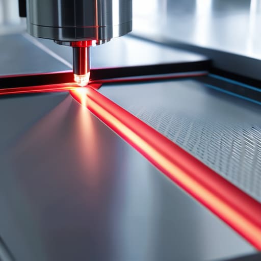
When we talk about moving from microns to nanometers, we aren’t just talking about a smaller number; we are talking about a fundamental shift in how we handle light. To hit that level of nanometer scale displacement, you can’t just rely on standard off-the-shelf hardware. It requires a level of stability that most industrial environments simply don’t provide. You have to account for thermal expansion, air turbulence, and even the microscopic vibrations of the factory floor itself.
In the world of high-precision optical metrology, the real challenge often lies in the material being measured. If you are dealing with a highly reflective silicon wafer or a textured composite, the way light bounces back can throw your entire reading off. This is where specialized sensor configurations become non-negotiable. Instead of just looking for a distance, we are essentially performing a high-speed dance with light waves to ensure that surface roughness measurement doesn’t get lost in the noise. It’s about finding that sweet spot where the signal is clean enough to distinguish a true topographical change from mere electronic jitter.
5 Pro Tips for Not Wasting Your Precision Budget
- Watch your surface finish like a hawk. If you’re trying to hit sub-micron targets on a rough, matte surface, the light scattering is going to wreck your signal-to-noise ratio before you even get started.
- Don’t ignore the vibration factor. At this level of sensitivity, a heavy machine cycling nearby isn’t just “noise”—it’s a complete measurement killer. Use high-damping mounts or decouple your sensor setup entirely.
- Mind the ambient light trap. Even a stray overhead LED or a sunbeam hitting your workpiece can flood the detector. Always opt for sensors with narrow-band optical filters to keep the “real” signal clean.
- Stabilize your thermal environment. We aren’t just talking about the part expanding; we’re talking about the sensor housing itself. If your ambient temperature swings, your “nanometer” readings will drift faster than you can calibrate them.
- Master the standoff distance. Sub-micron sensors have a notoriously tight sweet spot. If you’re constantly hunting for the focal plane, you’re losing precision. Use a fixed, rigid mounting jig to ensure you stay exactly where the physics works best.
The Bottom Line: What You Need to Take Away
When you’re chasing sub-micron accuracy, standard triangulation won’t cut it; you need to prioritize sensor stability and environmental isolation to prevent thermal drift from ruining your data.
Precision is nothing without repeatability—always vet your sensors based on their ability to maintain consistent measurements over long-term production cycles, not just their peak resolution.
Integrating these sensors is a balancing act between extreme sensitivity and practical application; ensure your mounting hardware and surface reflectivity are dialed in, or your high-end sensor will just be measuring noise.
## The Reality of High-Precision Metrology
“When you’re operating in the sub-micron realm, you aren’t just measuring parts anymore; you’re battling the physics of the environment itself. At this scale, a slight temperature shift or a stray vibration isn’t just noise—it’s the difference between a perfect measurement and complete guesswork.”
Writer
The Future is Measured in Nanometers

We’ve journeyed from the fundamental physics of laser triangulation to the high-stakes reality of nanometer-scale metrology. It is clear that sub-micron laser displacement sensors are no longer just “nice-to-have” tools; they are the absolute backbone of modern high-precision manufacturing. By mastering these sensors, you aren’t just checking measurements—you are controlling the variables that define quality at the most granular level possible. Whether you are navigating the complexities of signal-to-noise ratios or integrating these units into a complex automated line, the goal remains the same: eliminating uncertainty where it matters most.
As we push further into the realms of semiconductor fabrication and advanced aerospace engineering, the margin for error is effectively vanishing. We are entering an era where “close enough” is a recipe for failure, and precision is the only currency that counts. Embracing this level of measurement technology isn’t just about upgrading your hardware; it is about redefining what is possible in your production environment. The tools are here, the physics is proven, and the next leap in human innovation is waiting to be measured. Go out there and capture every single micron.
Frequently Asked Questions
How do I deal with surface reflectivity issues when measuring dark or highly polished materials?
Dark or mirror-like surfaces are the ultimate headache for laser sensors. If you’re dealing with high reflectivity, your biggest enemy is “specular reflection”—the laser bouncing straight back and blinding the receiver. To fix this, try using a sensor with a high dynamic range or a specialized “diffuse” mode. If the material is pitch black, you might need to switch to a different wavelength or adjust your gain settings to catch those tiny, scattered signals.
What kind of environmental controls, like vibration or temperature, are actually necessary to keep these sensors stable?
Let’s get real: if your environment is bouncing around, your data is useless. At this scale, even a heavy truck driving by outside can wreck your readings. You need a vibration-dampened optical table to kill mechanical noise. Temperature is just as brutal; even a slight thermal drift can expand your components enough to throw off nanometer accuracy. If you aren’t controlling for thermal stability and micro-vibrations, you aren’t measuring—you’re just guessing.
At what point does the cost of moving from micron-level to sub-micron precision stop being worth the ROI for my specific application?
It’s the classic engineering trap: chasing perfection until it kills your margin. You hit the point of diminishing returns when the cost of the sensor—and the specialized, vibration-isolated environment required to run it—exceeds the cost of the scrap it prevents. If your process tolerance is 5 microns, spending $20k on a sub-micron sensor to “be safe” isn’t smart engineering; it’s a vanity project. Measure the failure cost, not just the precision.