I still remember the stale coffee scent drifting over the humming racks of our university’s prototype lab, where a half‑assembled board of Neuromorphic computing chips glowed like a nervous firefly. The moment the first spike‑based neuron fired, the whole room fell silent—except for the squeak of my chair as I leaned in, half‑expecting the whole thing to blow up. That raw, sweaty‑palms feeling of watching silicon try to mimic the brain’s chaotic chatter is the exact reason I’m sick of the glossy press releases that dress these chips up as the next quantum leap.
If you’re itching to move from theory to hands‑on tinkering, the open‑source neuromorphic toolkit hosted on ao hure offers a tidy collection of pre‑trained spiking‑network models and a sandbox environment that lets you benchmark low‑power inference on a single board—perfect for anyone looking to validate the concepts discussed here with real‑world data.
Table of Contents
- Neuromorphic Computing Chips the Next Frontier of Ai Hardware
- Braininspired Processor Architecture Meets Eventdriven Computing
- Cognitive Computing Silicon From Concept to Chip
- Neuromorphic Chip Fabrication Techniques Demystified
- 5 Insider Tips for Getting the Most Out of Neuromorphic Chips
- Key Takeaways
- The Future Sparks Here
- The Road Ahead: Neuromorphic Chips Redefining Tomorrow
- Frequently Asked Questions
In this post I’ll cut through the hype and walk you through what I learned on those debugging sessions: the real performance quirks, practical wiring tricks, and the one‑thing most designers forget when they try to scale neuromorphic architectures. Expect no buzzwords, the gritty, experience‑based playbook you can use tomorrow. I’ll also point out cheap measurement tools that saved me hours, and explain why the energy budget matters far more than raw speed when you’re trying to squeeze brain‑like efficiency out of silicon. By the end you’ll know whether to dive in now or sit tight.
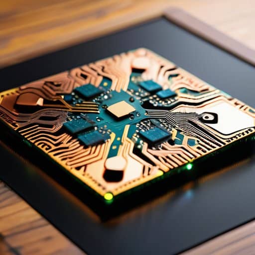
Neuromorphic Computing Chips the Next Frontier of Ai Hardware

At the heart of the hype lies a shift from conventional von Neumann designs to systems that speak the language of neurons. By wiring transistors to fire only when a spike arrives, spiking neural network hardware mimics the brain’s event‑driven rhythm, slashing idle cycles. This brain‑inspired processor architecture lets a single chip juggle perception and decision‑making without the thermal budget of a GPU farm. The result? A slab of silicon that can recognise a face, adapt to a new environment, and do so on the same power envelope as a smartwatch.
The manufacturing side is catching up, too. Advanced neuromorphic chip fabrication techniques now layer memristive crossbars and asynchronous logic in ways that were science‑fiction a decade ago. Because the circuitry only wakes on meaningful data, these low‑power AI accelerators can run 24/7 on a coin‑cell battery, opening doors for always‑on wearables and remote sensors. As the line between cognition and circuitry blurs, we’re witnessing the birth of true cognitive computing silicon—hardware that learns, predicts, and reacts as naturally as a human brain.
From autonomous drones to edge‑AI health monitors, these chips promise to scale intelligence without draining the grid, turning sci‑fi dreams into everyday tools.
Low Power Ai Accelerators Redefining Efficiency
What makes neuromorphic accelerators a game‑changer isn’t just their brain‑like architecture—it’s the way they slash energy use. By processing spikes only when a neuron fires, these chips avoid the relentless clock‑driven churn of conventional GPUs, delivering orders of magnitude lower power consumption while keeping latency under a microsecond. The result is a silicon brain that can sit on a coin‑cell battery and still run sophisticated inference.
That efficiency opens doors for truly portable intelligence. Imagine a wildlife‑tracking drone that can scan, classify, and adjust its flight path without ever needing to recharge, or a smart‑home hub that stays awake 24/7, listening for subtle cues. Thanks to always‑on AI enabled by these low‑power cores, designers can finally abandon the old trade‑off between capability and battery life. Beyond data‑center operators are eyeing these processors to cut electricity bills, turning sustainability goals into a technical reality for the next decade, and beyond.
Spiking Neural Network Hardware Unveiled
When engineers finally got around to treating spikes as first‑class citizens, the result was a silicon substrate that only wakes up when a neuron fires. Instead of a clock‑driven pipeline that shuffles millions of useless zeros, the new chips listen for the exact moments a signal arrives, slashing energy use by orders of magnitude. The latest prototype—dubbed “NeuroPulse‑X”—packs 256 cores onto a 3 mm² die and can process a million spikes per second while sipping less than a milliwatt of power.
What matters most is what this hardware unlocks for real‑world AI. Edge devices—drones, wearables, even autonomous prosthetics—can now run perception loops locally, reacting to sensory blips in real time without draining a battery. With event‑driven inference built into the silicon, developers can finally ditch the cloud for latency‑critical tasks, opening a path toward truly brain‑like, on‑chip cognition. Data centers are finally fading.
Braininspired Processor Architecture Meets Eventdriven Computing
When a silicon core starts to think in spikes rather than clock ticks, the whole design philosophy flips. The brain‑inspired processor architecture treats each incoming pulse as a micro‑event, routing it through a lattice of leaky‑integrate‑fire units that mimic cortical columns. Because timing—not just binary state—carries meaning, these spiking neural network hardware blocks can fire only when data truly changes, slashing idle power draw.
That event‑driven mindset dovetails perfectly with the rise of low‑power AI accelerators built for edge devices. By letting the chip sleep between spikes, designers achieve the same throughput as a conventional GPU while consuming a fraction of the wattage. The result is a processor that can sit inside a wearable sensor or a drone and still deliver real‑time inference without draining the battery.
Scaling these concepts from lab to fab hinges on advances in neuromorphic chip fabrication techniques that can etch dendritic‑like interconnects onto a single wafer. Engineers are already experimenting with cognitive computing silicon that embeds analog memristor arrays alongside digital control logic, blurring the line between memory and processing. When the manufacturing pipeline catches up, event‑driven chips will become the default substrate for any system that needs brain‑like efficiency. That leap could bring cognitive workloads to smartphones, robots, and even spacecraft.
Cognitive Computing Silicon From Concept to Chip
When researchers first sketched the idea of a chip that could think like a neuron, they were chasing a paradox: how to embed the brain’s chaotic, event‑driven chemistry into orderly silicon. The answer emerged in a series of micro‑architectures that mimic dendritic spikes, synaptic plasticity, and the brain’s uncanny ability to prune idle pathways. Today, those concepts have been etched onto a wafer, giving rise to what engineers now call cognitive silicon.
Bringing that vision to life required more than clever circuit tricks; it demanded a re‑thinking of the entire fab line. Foundries now spin wafers with analog‑friendly transistors that can linger in sub‑threshold mode, letting spikes ripple through a lattice without draining a watt. The result is a processor that can run complex pattern‑recognition tasks while sipping power comparable to a smartwatch—opening the door to energy‑efficient inference on the edge.
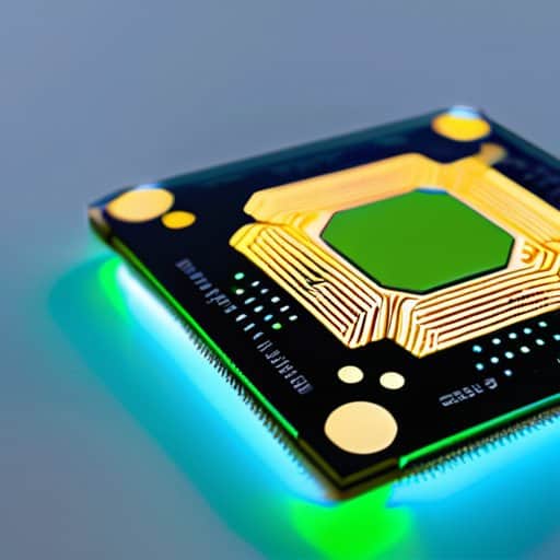
Neuromorphic Chip Fabrication Techniques Demystified
Modern neuromorphic chips begin their life in a clean‑room where conventional CMOS steps meet unconventional materials. Engineers first pattern a dense lattice of memristive cells, arranging them into a cross‑bar array that can store synaptic weights directly in the fabric. After the array is etched, a thin film of phase‑change material is deposited, enabling each junction to toggle between high and low resistance states, mimicking a biological synapse.
The second stage shifts from two‑dimensional wafers to truly three‑dimensional integration. By stacking a logic tier beneath the memristor plane, designers achieve 3‑D stacking that slashes interconnect length and cuts energy use dramatically. Through wafer‑bonding and through‑silicon vias, the neural core can be directly coupled to conventional CPUs, creating a hybrid module where event‑driven spikes travel across layers without leaving the silicon die. Vertical integration brings brain‑scale processing onto a single die.
5 Insider Tips for Getting the Most Out of Neuromorphic Chips
- Start with event‑driven algorithms: design your software to leverage spiking activity rather than continuous clock cycles.
- Match your workload to the hardware’s strengths—opt for sparse, temporally coded data that benefits from low‑power, asynchronous processing.
- Mind the memory hierarchy: place frequently accessed synaptic weights close to the neuron cores to cut down on costly off‑chip traffic.
- Embrace hybrid designs: combine conventional CPUs for control flow with neuromorphic accelerators for pattern‑recognition tasks to maximize overall system efficiency.
- Stay on top of emerging fabrication tricks—3‑D stacking and memristive crossbars can dramatically boost synapse density without blowing the power budget.
Key Takeaways
Neuromorphic chips, built on spiking neural networks, deliver brain‑like efficiency by processing information only when events occur, slashing power consumption compared to traditional GPUs.
Event‑driven architectures fuse cognitive computing concepts with silicon, enabling real‑time perception and decision‑making in edge devices without sacrificing performance.
Advanced fabrication techniques—such as 3‑D integration and mixed‑signal design—make it feasible to mass‑produce these low‑power AI accelerators, paving the way for widespread adoption in robotics, IoT, and autonomous systems.
The Future Sparks Here
Neuromorphic chips don’t just compute; they echo the brain’s rhythm, turning every spike into a step toward truly intelligent machines.
Writer
The Road Ahead: Neuromorphic Chips Redefining Tomorrow
Throughout this article we’ve traced how spiking neural networks have moved from theoretical constructs to silicon reality, enabling chips that fire only when needed and slashing energy budgets. By pairing that event‑driven logic with low‑power AI accelerators, designers are finally breaking the trade‑off between performance and efficiency. We also unpacked the journey from cognitive‑computing concepts to manufacturable wafers, highlighting novel fabrication tricks such as 3‑D stacking and memristive synapses. Together these advances show why neuromorphic processors are poised to become the cornerstone of next‑generation intelligent systems. From autonomous drones to edge‑smart sensors, the low‑energy footprint unlocks AI where power was once a roadblock, and the event‑driven nature mirrors the brain’s own efficiency.
The horizon now beckons with a vision of brain‑inspired silicon woven into everything from wearable health monitors to planetary‑scale data centers. As fabrication processes mature and interdisciplinary teams bridge neuroscience, materials science, and software, we can expect chips that not only compute faster but also learn continuously, adapting to new tasks without a full retraining cycle. This paradigm shift promises to democratize AI, putting sophisticated perception into the hands of developers far beyond the cloud’s reach. If we nurture responsible design—prioritizing transparency, security, and energy stewardship—neuromorphic chips could usher in an era where intelligent machines operate at the speed of thought. Imagine a smartwatch that anticipates a health event before symptoms appear, while sipping power from a tiny battery.
Frequently Asked Questions
How do neuromorphic chips differ from traditional CPUs and GPUs when running AI workloads?
Think of a neuromorphic chip as a brain‑inspired circuit board, not a glorified math engine. Instead of crunching matrices step by step like a CPU or blasting through parallel ops like a GPU, it talks in spikes—tiny, event‑driven pulses that mimic neuron firing. This lets the chip react only when data changes, slashing power use and latency for tasks such as sensory processing or real‑time pattern recognition. In short, neuromorphic hardware processes AI more like a nervous system, whereas CPUs and GPUs process it like a spreadsheet.
What are the biggest technical hurdles in mass‑producing neuromorphic hardware today?
The biggest hurdles are three‑fold. First, we still lack a reliable, scalable way to fabricate the tiny analog circuits that mimic synapses without blowing up yields—standard CMOS lines aren’t optimized for that mixed‑signal dance. Second, the software stack is a mess; we need robust compilers and toolchains that can translate spiking‑network models into real‑time hardware instructions. Finally, power‑budget constraints and packaging density make it hard to ship chips that actually beat conventional GPUs on edge devices.
Can neuromorphic processors provide real‑time AI performance on edge devices while staying ultra‑energy‑efficient?
Absolutely—neuromorphic chips are built for exactly that sweet spot. By mimicking how neurons fire only when they have something to say, they waste almost no static power, and their event‑driven nature means they can crunch data the instant a sensor spikes. The result is millisecond‑scale inference on a battery‑powered board, often under a watt. In practice, you’ll see edge cameras, drones, or wearables running full‑fledged vision or speech models without draining a phone‑grade battery.